Like other electronic devices, cell phones have undergone many advancements in the many years of their existence.
However, a cellphone’s difference is its many added utilities that have made it more popular for use. The cellphone has been transformed from just a communication device to a device with an almost endless possibility.
With added utilities, including cameras, music players, and even scanners, the cellphone has become a necessary luxury.
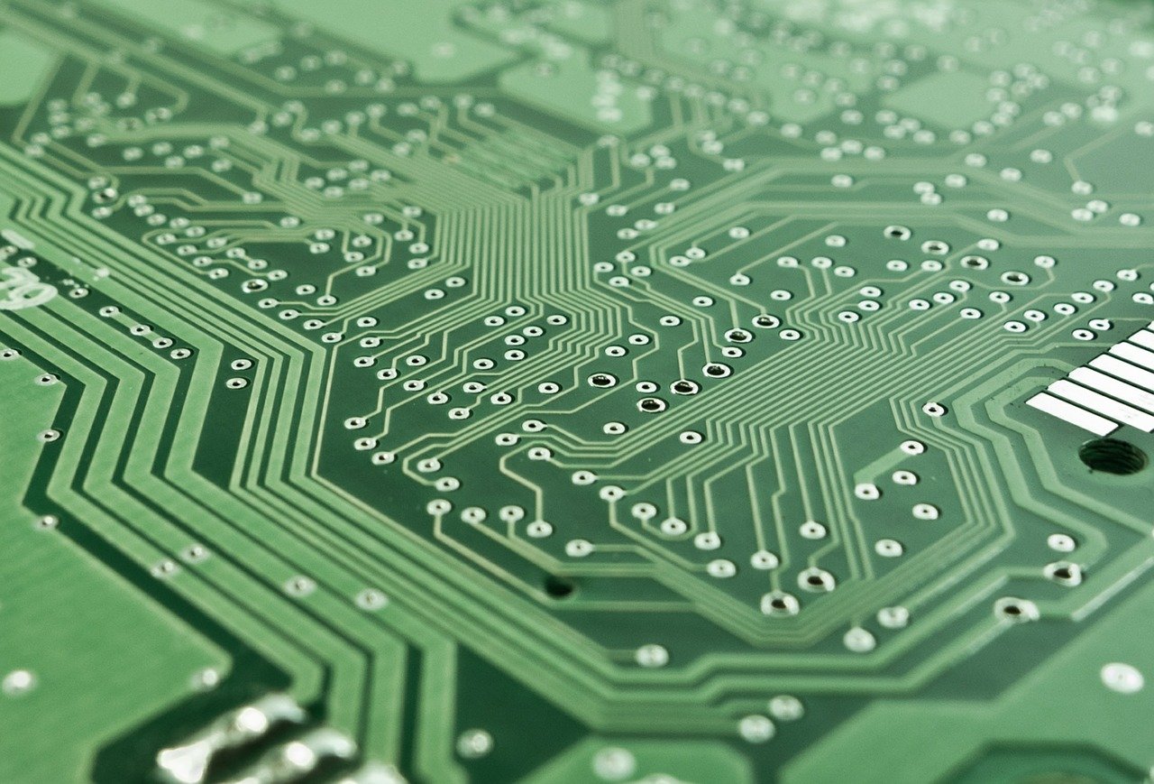
This increased function impacts the PCBs (Printed Circuit Boards), accommodating these additional components as tiny elements connect on sometimes small or layered PCBs.
Hence, there is the need to properly ascertain the integrity of these components’ connections on the PCBs.
However, X-ray machines are mostly automated and can be modified to suit different inspection specifications.
One technology that has seen increased use for inspecting the integrity of PCB connections is X-ray technology. PCB X-ray inspection has enjoyed popularity in assessing cellphone’s PCBs because it can identify various defects even when hidden from the ordinary eye.
Workings of PCB X-ray inspection
When inspecting PCBs using X-ray technology, skilled technicians often pass the samples through the rays generated from an X ray machine.
This machine is a piece of industrial radiography equipment similar in principle to the X-ray equipment used in the medical field to scan human bones for fracture.
This Industrial radiography equipment generates radiations from an X-ray tube to penetrate the hidden parts and layers of the PCB and to locate flaws present within the board.
Nonetheless, a specified threshold dose is vital for the radiation generated. This dose should stay within the threshold so that it does not cause additional errors to the already present ones – if there are any errors.
The radiation then projects an image of the samples on a screen for onward analysis and identification of the defects using computer programs.
Defect detection using X-ray inspection
X-ray machine price is usually not a big deal since several imperfections can be identified when conducting PCB X-ray inspection. The ones that are often encountered are highlighted below.
- Registration defects occur due to misalignment of components with pads or solder balls on BGA (Ball Grid Array) systems. Computer analysis of the X-ray image can quickly identify this critical flaw employing image magnification and enhancement processes.
- A missing connection happens when either the solder is misplaced on the PCB or the solder balls are absent on the BGAs. Rough handling and packaging mishandling can usually cause missing connections.
- Voids in solder is another possible error that PCB X-ray inspection can easily detect. Solder joints can contain voids due to overheating of trapped compounds within the solder. This void may result in process failure later on.
- Wrong solder placement often occurs when a solder ball is removed but not properly dislodged from the BGA. This misplaced solder ball often finds itself under or around another component leading to a possible bridging problem.
- Inadequate solder connection is encountered due to insufficient flow of solder to establish proper contact between the PCB and components. A cold solder joint can also lead to unsatisfactory solder connection if the flow heat required for the solder is not sufficient.
- Solder Bridges are putting an excessive quantity of solder on one or more PCB contacts. It also occurs when solder balls are delivered to the wrong contacts on the PCB.
An X-ray inspection will identify such errors as dark spots even though no mark is expected in those areas.
Identification of this flaw using X-ray inspection prevents failures that might occur during a power-up test of the PCB.
- The open connection will occur if there is no link between the solder and the pad contacts. This flaw might be attributed to inadequate melting of solders of one end, or both ends of a BGA, resulting in a loss of connection.
- Misaligned and missing components on PCB are placement errors that X-ray inspection can detect using polarization. A polarized capacitor, for instance, has an orientation that X-rays can check to confirm if it is right using its offset punch.
All these detection capabilities justify its benefits when considering X-ray machine price.
Final Take
The role of PCB X-ray inspection in ascertaining the integrity and quality of PCBs produced for cellphones cannot be overemphasized. This role has many merits that have made it popular in the electronic industry as the preferred method or inspection tool.
However, a critical look at the PCB manufacturer’s need is essential in choosing the best X-ray inspection solution that is well-suited to meet this need.
This analysis is needed because X-ray inspection solution providers have developed a wide variety of X-ray systems.
These systems can range from basic to well-advanced ones. They can carry functions that may include 2D or 3D imaging, single or multiple sampling production lines, and manual or automatic solution systems.


 Bitcoin
  Ethereum
  Tether
  XRP
XRP  Solana
  USDC
USDC  TRON
TRON  Cardano
  Lido Staked Ether
  Toncoin
  Avalanche